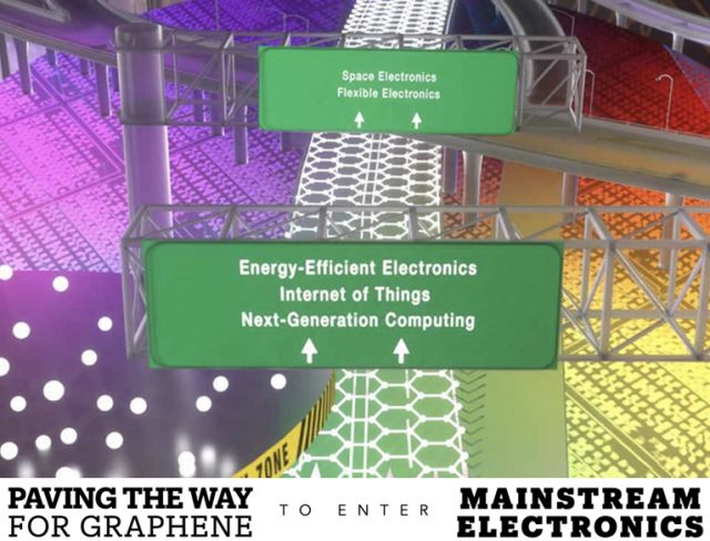
Kaustav Banerjee "Paving the Way for Graphene"
Banerjee's NRL lab develops an innovative synthesis process, overcoming a stubborn obstacle to wide-scale deployment of graphene in the semiconductor industry
Electrical & Computer Engineering Prof. Banerjee's NRL lab develops an innovative synthesis process, overcoming a stubborn obstacle to wide-scale deployment of graphene in the semiconductor industry
Ever since graphene, the flexible, two-dimensional form of graphite (think of a 1-atom-thick sheet of pencil lead),was discovered in 2004, researchers around the world have been working to develop commercially scalable applications for this incredibly high-performance material.
Graphene is 100 to 300 times stronger than steel and has a maximum electrical current density orders of magnitude greater than that of copper, making it the strongest, thinnest, and, by far, the most reliable electrically conductive material in the world. This is why it is an extremely promising material for interconnects, the fundamental components that connect billions of transistors on microchips in computers and other electronic devices in the modern world.
For over two decades, interconnects have been made of copper, but that metal encounters fundamental physical limitations as electrical components that incorporate it shrink to the nanoscale. “As you reduce the dimensions of copper wires, their resistivity shoots up,” says Kaustav Banerjee, professor in the Department of Electrical and Computer Engineering at UC Santa Barbara’s College of Engineering. “Resistivity is a material property that is not supposed to change, but at the nanoscale, all properties change.”
As the resistivity increases, copper wires generate more heat, reducing their current carrying capacity. It’s a problem that poses a fundamental threat to the $500 billion semiconductor industry. Graphene has the potential to solve that and other issues, but a major obstacle is designing graphene micro-components that can be manufactured on-chip on a large scale in a commercial foundry.
“Whatever the component, be it inductors, interconnects, antennas, or anything else you want to do with graphene, industry will move forward with it only if you find a way to synthesize graphene directly onto silicon wafers,” Banerjee says. He explains that all the manufacturing processes related to the transistors, which are made first, are referred to as the ‘front end.’ To synthesize something at the back-end, that is, after the transistors are fabricated, you face a tight thermal budget, such that you cannot exceed a temperature of about 500 degrees Celsius. If the silicon wafer gets too hot during the back-end processes employed to fabricate the interconnects, the other elements that are already on the chip may get damaged, or some impurities may start diffusing, changing the characteristics of the transistors.”
Now, after a decade-long quest to achieve graphene interconnects, Banerjee’s lab has developed a method to implement high-conductivity nanometer-scale doped multilayer graphene (DMG) interconnects that are compatible with high-volume manufacturing of integrated circuits. A paper describing the novel process was selected as one of the top papers from more than 230 accepted for oral presentations at the 2018 IEEE International Electron Devices Meeting (IEDM), and was one of only two papers included in the first annual “IEDM Highlights” section of the December 2018 issue of the journal Nature Electronics.
COE Convergence – "Paving the Way for Graphene" (full article on pg. 31)